An NE555 in astable mode repeatedly charges and discharges a capacitor, producing a free-running rectangular signal. The calculator above works in both directions: enter known component values to obtain the timing, or enter a target frequency and duty cycle to search nearby E24 resistor and E12 capacitor values.
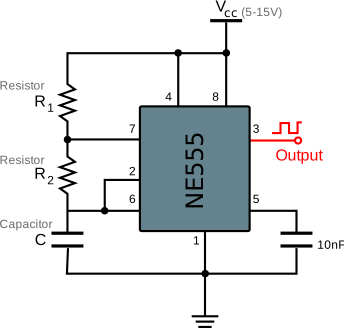
How the Astable Cycle Works
The timing capacitor is connected to the trigger and threshold inputs. While the discharge transistor is off, the capacitor charges toward the supply through both resistors, so the charging resistance is
\[ R_{\mathrm{charge}}=R_1+R_2. \]
When the capacitor reaches the upper comparator threshold, approximately \(2V_{CC}/3\), the output changes state and the internal discharge transistor turns on. The capacitor then discharges through \(R_2\) alone until it reaches the lower threshold, approximately \(V_{CC}/3\). The discharge transistor turns off and the cycle starts again.
Where the \(\ln 2\) Factor Comes From
A capacitor charging from an initial voltage \(V_0\) toward a final voltage \(V_S\) through a resistance \(R\) follows
\[ V_C(t)=V_S-(V_S-V_0)e^{-t/(RC)}. \]
For the high interval, \(V_0=V_{CC}/3\), \(V_S=V_{CC}\), and the transition occurs at \(V_C=2V_{CC}/3\). Substitution cancels the supply voltage:
\[ \frac{2}{3}=1-\frac{2}{3}e^{-t_H/((R_1+R_2)C)}, \qquad e^{-t_H/((R_1+R_2)C)}=\frac{1}{2}. \]
Taking the natural logarithm gives
\[ t_H=\ln(2)(R_1+R_2)C. \]
Discharging from \(2V_{CC}/3\) to \(V_{CC}/3\) through \(R_2\) produces the same voltage ratio and therefore the same logarithmic factor:
\[ t_L=\ln(2)R_2C. \]
Period, Frequency, and Duty Cycle
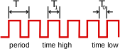
One complete period is the sum of the high and low intervals:
\[ T=t_H+t_L=\ln(2)(R_1+2R_2)C, \qquad f=\frac{1}{\ln(2)(R_1+2R_2)C}. \]
The fraction of the period spent high is
\[ D=\frac{t_H}{T}=\frac{R_1+R_2}{R_1+2R_2}. \]
For positive resistor values, \(R_1+R_2\) is always greater than half of \(R_1+2R_2\). The classic two-resistor topology therefore has \(D>50\%\). It approaches 50% only as \(R_1/R_2\) approaches zero; it cannot produce an exact 50% duty cycle with two positive timing resistors. A steering diode or a different oscillator topology is needed when independent charge and discharge paths are required.
Using the Reverse Calculator
The reverse search evaluates E24 resistor values and E12 capacitor values over practical ranges. Every candidate is calculated with the same timing equations, then ranked by the combined relative frequency error and duty-cycle error. Clicking a row copies that component set into the direct calculator.
A requested duty cycle must lie strictly between 50% and 100%. Very high duty cycles require \(R_1\) to dominate \(R_2\), while values close to 50% require \(R_2\) to be much larger than \(R_1\). The optional 1 kΩ limit is a conservative design aid rather than a universal device rating; the permitted discharge current and resistor limits must be checked against the data sheet for the exact 555 variant and supply voltage.
Limits of the Ideal Calculation
The equations assume exact comparator thresholds, zero discharge-transistor saturation voltage, no propagation delay, and ideal resistors and capacitors. Real frequency and duty cycle are affected by component tolerance, capacitor leakage and dielectric behavior, threshold variation, temperature, supply voltage, output loading, and the bipolar or CMOS implementation of the timer.
At long periods, capacitor leakage can become comparable to the timing current. At high frequencies, internal delays and finite output transition times become significant. Use the calculated result as a nominal design point, then verify the operating range with worst-case component values and the electrical characteristics in the selected device's data sheet.